- 您现在的位置:买卖IC网 > Sheet目录479 > MRF89XA-I/MQ (Microchip Technology)TXRX ISM SUB-GHZ ULP 32QFN
�� �
�
�MRF89XA�
�2.9.1�
�TRANSMITTER� ARCHITECTURE�
�In� OOK� mode,� the� phase� difference� between� the� I� and�
�Figure� 2-6� illustrates� the� transmitter� architecture� block�
�diagram.� The� baseband� I� and� Q� signals� are� digitally�
�generated� by� a� DDS� whose� Digital-to-Analog�
�Converters� (DAC)� followed� by� two� anti-aliasing� low-�
�pass� filters� transform� the� digital� signal� into� analog� in-�
�phase� (I)� and� quadrature� (Q)� components� whose�
�frequency� is� the� selected� frequency� deviation,� is� set�
�using� the� FDVAL<7:0>� bits� from� FDEVREG<7:0>.�
�In� FSK� mode,� the� relative� phase� of� I� and� Q� is� switched�
�by� the� input� data� between� -90°� and� +90°� with� continu-�
�ous� phase.� The� modulation� is� therefore� performed� at�
�this� initial� stage,� because� the� information� contained� in�
�the� phase� difference� will� be� converted� into� a� frequency�
�shift� when� the� I� and� Q� signals� are� up-converted� in� the�
�first� mixer� stage.� This� first� up-conversion� stage� is� dupli-�
�cated� to� enhance� image� rejection.� The� FSK� convention�
�is� such� that:�
�DATA� =� 1� →� f� rf� +� f� dev�
�DATA� =� 0� →� f� rf� –� f� dev�
�Q� channels� is� kept� constant� (independent� of� the�
�transmitted� data).� Thus,� the� first� stage� of� up-conversion�
�creates� a� fixed� frequency� signal� at� the� low� IF� =� f� dev� (this�
�explains� why� the� transmitted� OOK� spectrum� is� offset� by�
�f� dev� ).� OOK� Modulation� is� accomplished� by� switching� the�
�PA� and� PA� regulator� stages� ON� and� OFF.� By�
�convention:�
�DATA� =� 1� →� PAon�
�DATA� =� 0� →� PAoff�
�After� the� interpolation� filters,� a� set� of� four� mixers�
�combines� the� I� and� Q� signals� and� converts� them� into� a�
�pair� of� complex� signals� at� the� second� intermediate�
�frequency,� equal� to� one-eighth� of� the� LO� frequency,� or�
�one-ninth� of� the� RF� frequency.� These� two� new� I� and� Q�
�signals� are� then� combined� and� up-converted� to� the�
�final� RF� frequency� by� two� quadrature� mixers� fed� by� the�
�LO� signal.� The� signal� is� pre-amplified,� and� then� the�
�transmitter� output� is� driven� by� a� final� power� amplifier�
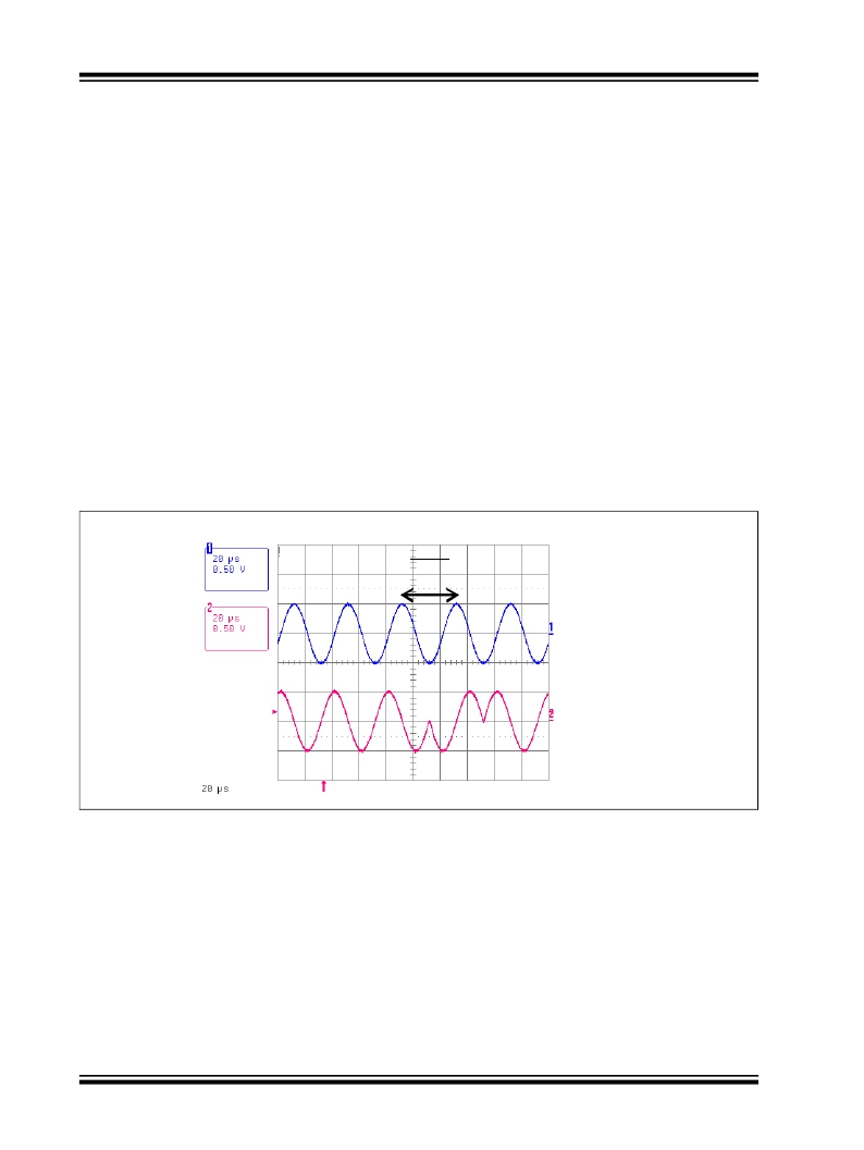
�stage.� The� I� and� Q� signal� details� are� illustrated� in�
�Figure� 2-7� .�
�FIGURE� 2-7:�
�I(t),� Q(t)� Signals� Overview�
�1�
�Fdev�
�I(t)�
�Q(t)�
�DS70622C-page� 20�
�Preliminary�
�?� 2010–2011� Microchip� Technology� Inc.�
�发布紧急采购,3分钟左右您将得到回复。
相关PDF资料
MRF89XAM9A-I/RM
IC TXRX MOD 915MHZ ULP SUB-GHZ
MRX-001-433DR-B
MODULE RECEIVER 433MHZ 18DIP
MRX-002-433DR-B
MODULE RECEIVER 433MHZ 18DIP
MRX-002SL-433DR-B
MODULE RCVR 433MHZ SAW LN 24DIP
MRX-005-915DR-B
MODULE RECEIVER 915MHZ 18DIP
MRX-005SL-915DR-B
MODULE RCVR 915MHZ SAW LN 24DIP
MRX-007-433DR-B
MODULE RECEIVER 433MHZ 18DIP
MRX-008-433DR-B
MODULE RECEIVER 433MHZ 18DIP
相关代理商/技术参数
MRF89XAM8A-I
制造商:MICROCHIP 制造商全称:Microchip Technology 功能描述:Ultra Low-Power, Integrated ISM Band Sub-GHz Transceiver
MRF89XAM8A-I/RM
功能描述:射频模块 868MHz Sub-GHz transceiver module
RoHS:否 制造商:Linx Technologies 产品:Transceiver Modules 频带:902 MHz to 928 MHz 输出功率:- 15.5 dBm to + 12.5 dBm 接口类型:UART 工作电源电压:- 0.3 VDC to + 5.5 VDC 传输供电电流:38.1 mA 接收供电电流:22.7 mA 天线连接器类型:U.FL 最大工作温度:+ 85 C 尺寸:1.15 mm x 0.63 mm x 0.131 mm
MRF89XAM8A-I/RM
制造商:Microchip Technology Inc 功能描述:, Leaded Process Compatible:Yes, Peak Re
MRF89XAM9A_12
制造商:MICROCHIP 制造商全称:Microchip Technology 功能描述:915 MHz Ultra Low-Power Sub-GHz Transceiver Module
MRF89XAM9A-I/RM
功能描述:射频模块 915MHz Sub-GHz Transceiver Mod RoHS:否 制造商:Linx Technologies 产品:Transceiver Modules 频带:902 MHz to 928 MHz 输出功率:- 15.5 dBm to + 12.5 dBm 接口类型:UART 工作电源电压:- 0.3 VDC to + 5.5 VDC 传输供电电流:38.1 mA 接收供电电流:22.7 mA 天线连接器类型:U.FL 最大工作温度:+ 85 C 尺寸:1.15 mm x 0.63 mm x 0.131 mm
MRF89XAM9AT-I/RM
制造商:Microchip Technology Inc 功能描述:915 MHz Ultra Low-Power Sub-GHz Transceiver Module
MRF89XAT-I/MQ
功能描述:射频收发器 868/915/950 MHz Sub-GHz transceiver RoHS:否 制造商:Atmel 频率范围:2322 MHz to 2527 MHz 最大数据速率:2000 Kbps 调制格式:OQPSK 输出功率:4 dBm 类型: 工作电源电压:1.8 V to 3.6 V 最大工作温度:+ 85 C 接口类型:SPI 封装 / 箱体:QFN-32 封装:Tray
MRF8HP21080HR3
功能描述:射频MOSFET电源晶体管 HV8 2.1GHZ 160W NI780H-4 RoHS:否 制造商:Freescale Semiconductor 配置:Single 晶体管极性: 频率:1800 MHz to 2000 MHz 增益:27 dB 输出功率:100 W 汲极/源极击穿电压: 漏极连续电流: 闸/源击穿电压: 最大工作温度: 封装 / 箱体:NI-780-4 封装:Tray